|
|
|
|


|
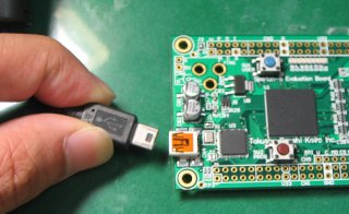
TOKUDEN Spartan-6 FPGA BoardTOKUDEN Spartan-6 Board is a cardsize FPGA evaluation board. This board is equipped with a DDR2 memory and an USB2.0 interface. You can configure FPGA through on-board USB-JTAG.
Summary
The difference with other brandsThis board is different from the FPGA evaluation board of other companies. This board is compact size and does not interfere. And because the communication with the PC is NOT Ethernet but USB, it is not necessary to use MicroBlaze and uCLinux.
Therefore the design of FPGA becomes simple and is overwhelmingly short at logic synthesize and place-and-route time. You do not have to wait at long time anymore to compile FPGA.
Furthermore, the JTAG cable is unnecessary because on-board High speed USB-JTAG and dedicated software are provided. You can begin FPGA development immediately and make efforts in a main profession. Without being bothered by ethernet and the Softcore CPU.
Product lineup and ordering information(1) TKDN-SP6-16 It equipped with a mass production Spartan-6, XC6SLX16-2CSG324C. The price is 37,800 JPY (excluding Japanese consumption tax).
(2) TKDN-SP6-45 It equipped with a mass production Spartan-6, XC6SLX45-2CSG324C. The price is 41,800 JPY (excluding Japanese consumption tax).
TKDN-SP6-45 can be purchased from a distributer Trenz Electronic. If you live in Europe or North America, please visit Trenz Electronic.
Or , if you want to order directly from us, please contact us . Our online shopping site is here. but this page is written in Japanese and payment method is bank transfer only.
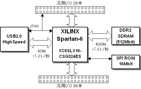
SpecificationsFPGA It is equipped with the newest FPGA 'Spartan-6' which has 324 pins. XC6SLX16 : 14,579 logic cells, 32 units of DSP48 slices, and 32 units of 18kbit Block RAM XC6SLX45 : 43,661 logic cells, 58 units of DSP48 slices, and 116 units of 18kbit Block RAM
* DDR2 SDRAM HYB18T512800BF-2.5 (Quimonda company) * 512Mbit(64Mword , 8 bit width, 4 bank) * Maximam operation speed 400MHz
* EZ-USB FX2LP CY7C68013A (Cypress Semiconductor) * Transfer of both application data and USB-JTAG is realized in same USB port. * Immediately usable IP core and device driver for EZ-USB FX2 are provided * Performance IN direction : Max 40MBytes/sec OUT direction : Max 30MBytes/sec (These speeds are fluctuates by the specifications of the PC to use.) * Onboard USB-JTAG and USB-JTAG-SPI programmer It takes about 3 seconds for programming XC6SLX16 It takes about 10 seconds for programming XC6SLX45 It takes about 30 seconds for programming SPI ROM AT45DB161D (for XC6SLX16 bitstream) It takes about 90 seconds for programming SPI ROM AT45DB161D (for XC6SLX45 bitstream)
SPI Flash memory * ATMEL's SPI Flash memory AT45DB161D (16Mbit size)
General purpose I/O * 28 I/Os are prepared upper side of the board. * 36 I/Os are prepared lower side of the board. * Total 29 pairs of differential signal are available. * You can mount on an universal board with 2.54mm pitch pin headder.
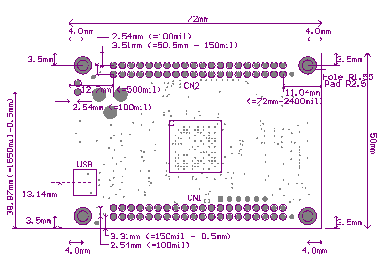
Board size 72mm x 50mm
Block diagram
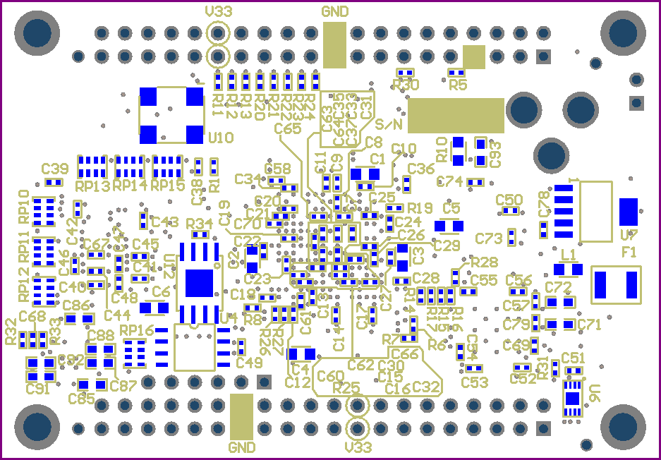
Board view and silk images
PINOUT of the board connector* CN2 (upper side) is connected to Bank0. * CN1 (lower side) is mainly connected to Bank2. IO_B0 to IO_B3 are conntected to Bank3. * Vref pin of Bank2 is connected to CN2. * Totak 29 differential pare signals are available. * Differential pair signals are routed as equivalent length (< 10mil).
(click to magnify)
Connector location
(click to magnify)
Download of free documentsThe following documents are downloadable freely. ・ ・ ・
Download of design resourcesThe following information are downloadable by a person who purchased. Please input LOGIN ID to download.
Complete schematics (all pages) ・
・
・
・
・
About sample designThe sample design communicate with an internal logic of FPGA via USB, The main function as follows.
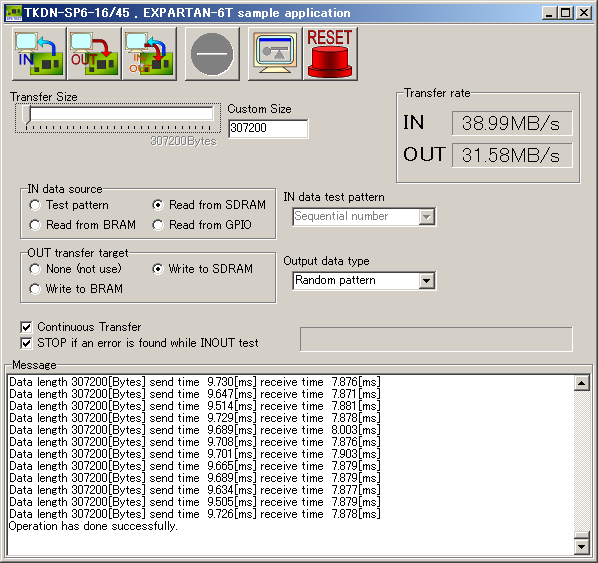
(1) USB operation test It can retrieve contents of test pattern , the DDR2 SDRAM, contents of BlockRAM and a current value of GPIO. Retrieved data can be shown as a VGA size (640x480) image.
(2) Testing DDR2 SDRAM It can read and write the data of the up to 64M byte via USB. You can send data from FILE and readback and show as a VGA Image.
(3) Open short test of I/O pin headder Among 64 I/O pin headers, one is H level and others become L level. (It is so-called walking '1') With an oscilloscope, open short test is possible. They become high impedance when reading from USB.
(4) LED display D7 indicates while DDR2 SDRAM read operation D8 indicates while DDR2 SDRAM write operation D1-D6 counts up while push switch SW1 is pushed.
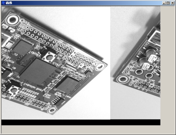
The sample design is controled with application software "sp6test.exe". A working image of sp6test.exe is shown in the following figure.
Troubleshoot of current sample design versionA clock to DDR2 memory is not output It is a trouble of happen only in ISE12.1. Please update to ISE12.2, or please use ISE11.5.
Some timing constraints are not met There does not seem to be the serias problem. We just improve design in order to solve this problem.
Some errors are occurred when IN/OUT testing of the DDR2 memory. Because reading timing of the DDR2 memory does not match the right position with our DDR2 core, We just improve design in order to solve this problem.
It becomes hot during operation
USB-JTAG programming tool for FPGA and SPI ROMBecause this board is equipped with high level USB-JTAG function, programming of FPGA and SPI ROM is very easy.
To use the on board USB-JTAG function, you use sp6jtag utility software.
To program FPGA, connect usb connector of this board to your PC and launch SP6JTAGW utility.
It takes about 3 seconds for FPGA of TKDN-SP6-16 , about 10 seconds for TKDN-SP6-45. It takes about 30 seconds for SPI ROM under TKDN-SP6-16 , about 100 seconds under TKDN-SP6-45. There is not needed converting from BitStream file to MCS file with using the XILINX iMPACT.
Application "LED photo sensor array"A demonstration. When I shade on the LED matrix with a hand, LED shines in rainbow color. This is an example which the LED is used as an optical sensor.
The LED emits light when an electric current flows. On the contrary, the voltage occurs when exposed by light. Therefore, the LED can act as an optical sensor.
FPGA measures the output value of LED optical sensor , calculates and controls the emission of light of the LED. The strength of emission of LED is controlled smoothly by delta-sigma DAC in FPGA.
Because the sensitivity of the brightness of human eyes has a nonlinearity, six built-in DSP48 blocks of Spartan-6 is used to implement the third function and revise this human eyes' nonlinearity. Linear and smooth control of the LED is realized in this way. LED Photo sensor array
Copyright(C) 2009 TokushuDenshiKairo Inc. All rights reserved. |
||||||||


 DDR2 SDRAM
 USB
USB